
IPC, a trade association that promotes the standardization of electronic equipment, defines three packing level standards for the sizes of footprints for electronic components: A, B, and C. The packing level defines how much extra space a footprint has, with A levels having the most extra space, and C having the least. Consequently, the packing level affects how closely together you can place parts, or how tightly packed they can be.
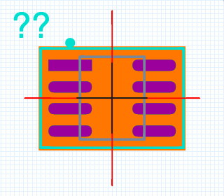
This animation demonstrates the effect of switching between the 3 difference packing levels on an SOIC-8 footprint.
For hand soldering, it’s a good idea to pack components loosely so that you have room to get at them with a soldering iron, meaning ‘A’ level is a good choice. For high-density, machine-assembled boards, a tight packing level is naturally a better choice.