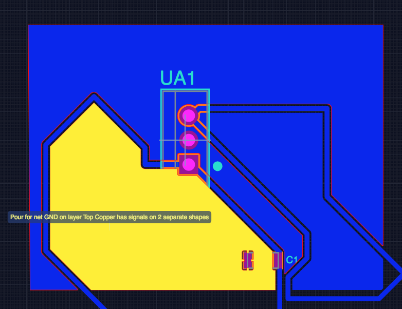
I have just poured the top copper on my board however I am getting a constraint saying "Pour for net GND on top copper has signals on 3 different shapes.
I am not sure what this means?

I have just poured the top copper on my board however I am getting a constraint saying "Pour for net GND on top copper has signals on 3 different shapes.
I am not sure what this means?
Hi @benpems
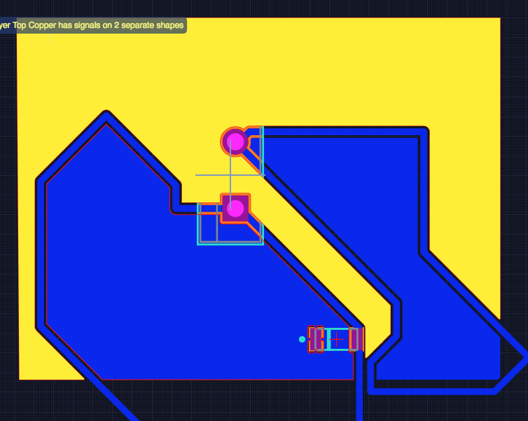
That is a design rule to let you know that you have a “split pour”. This means that you have traces that are disconnecting two or more section of the GND pour that you have in your design. This needs to be fixed before you go to manufacturing because your GND pins are not connected right now.
Hope this helps.
Below is a simple example of a split pour, I have highlighted 2 of the GND pour sections that are not connected.
Cheers,
Michael