Overlapping pour shapes create gaps

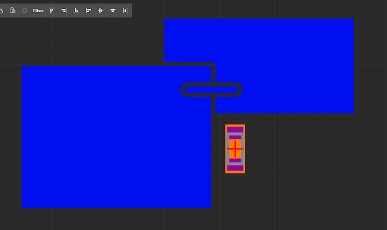
We have split our top ground pour in two, since our board requires different clearance distances applied to different sections of the board. We define them as overlapped. Even though the pours are associated with same named circuit (GND), we get a gap between the two pours.
None of the following settings appear to help:

  • assigning same pour priority and re-pouring them simultaneously
  • assigning different pour priorities and re-pouring them simultaneously
  • manually re-pouring one after the other
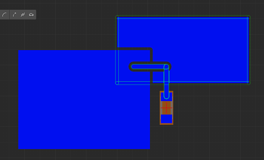
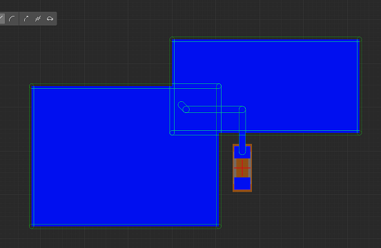
  • placing the pours adjacent to each other, ie back-to-back
  • toggling the island removal

It appears the pour tool is incorrectly adding the clearance distance between the two pours when it processes the 2nd pour.

As a workaround we may be able to manually place wide copper traces that span the gap, however we are concerned PCB manufacturer’s CAD tools may not correctly handle the resulting Gerbers. (We need a continuous GND plane for RF).

Other suggestions or a path to get a fix?

My suggestion is the following:

Start with the two pours seperated, with netlist say GND.

Proceed to repour both, you’ll notice the gap as per your post.
Next, grab a trace, and create a bridge between them. This is like your fix.
Next, extend the trace to connect also to a component with the same netlist.
In my diagram, I am extending it to the resistor top.
Finally repour all, and then remove the copper trace. You can alternatively leave it as well. It won’t impact anything.

image
image
image

I hope this helps.

Alternatively, you can just stay with your solution. The manufacturers might be okay with this, as they are used to having multiple coppers stacked to produce a final shape. They even have optimizer for this sort of thing, that will perform logical boolean operations on the shapes (or pours), before a final copper sheet is created.

One other way that just came to my head is, (which may or not be easier, depending on size and shape):

Pour each one separately, with the other completely offset from the original design by some known large amount, like 1000mil in the x direction. (Use the grid settings at 100mil, and arrow keys to move left/right by large amounts).

Then once you have each pour separately, simply overlap them.
Do not repour all -> this will break all your good work.

Just a thought.

Thanks Robert - the first suggestion (adding a trace to a component ground pad and then re-pouring all) does the trick.

I had tried something very similar, attaching the trace to a GND via, but that didn’t work.
Similarly, just adding a trace, but not connecting it to a component, breaks the first time one re-pours, since there isn’t any way to assign or edit a trace’s netlist.

As to your 2nd suggestion, not practical for my situation, as all the pour “cutouts” for
components in the shifted pour’s area would be incorrect.

Glad it helps :slight_smile: